Signal Chain ICs

PJ59555

Datasheet
Add to Consultation List

Product Description

Low Voltage 16-bit I2C and SMBus I/O Expander
with Interrupt

Product Features

Operation Voltage: 1.65V to 5.5V
StandbyCurrent: 3.5μA(Max. 5.5V)
5.5VTolerance I/O Port
Remote16-bit GPIO Expander
Compatible with SMBus and I2C interface
I2C Speed up to 1.0 MHz ( Fast-mode Plus )
Up to 8 slave addresses
Open-drain Interrupt output with active low to indicate input state changed.
Input, Output, and Configuration Register
Polarity Inversion Register
Built-in Power-on Reset
NoGlitch during Power-up
NoiseFilter on SCL/SDAinputs
16I/O pins:AsInputwith internal 100k pull-up resistor(default),AsOutputwithinternal push-pull
Latch feature when driving LEDs directly:with high current capability
Temperature Range:-40°C to 85°C

Product Introduction

Product Specifications

Related Files

Consultation List

Product Introduction

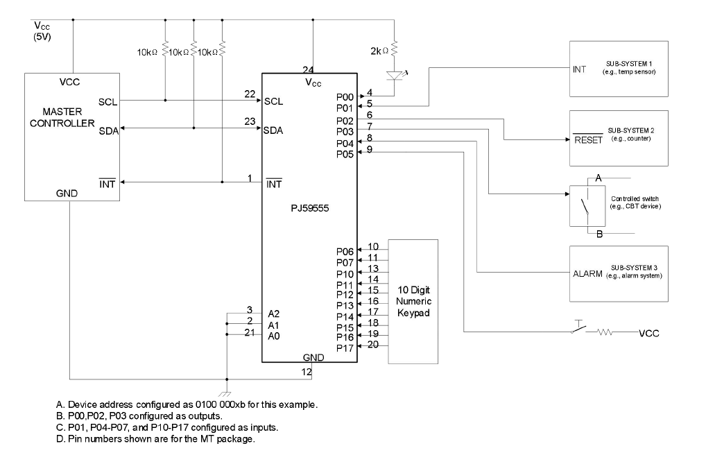
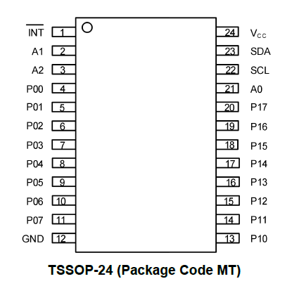
The chip is a 16-bit I/O expander. It provides remote GPIO expansion for most MCU families via the I2C or SMBus interface. The PJ59555 has two 8-bit Input Port register, Output Port register, Configuration register (setup as input or output), and Polarity Inversion register (active high or active low). After power on, the 16 I/O pins are configured as inputs with an internal weak pull up to VCC. However, the master can enable the I/O pins as either inputs or outputs individually by setup the configuration register bits. If no external signals are applied to the PJ59555 I/O pins, the voltage level is high due to the internal pull-up resistors. The data for each input or output is stored in the corresponding input or output port register. The polarity of the Input Port register can be inverted with the Polarity Inversion register. The master can reset the chip probably caused by timeout or other improper operation using the power-on reset feature, which resets all registers in their default state and initializes the I2C/SMBus state machine. The chip has outputs latch feature, which can protect the chip when driving LEDs directly with high-current capability. The PJ59555 open-drain interrupt output is activated when any input state differs from its corresponding Input Port register state and is used to indicate to the system master that an input state has changed. Available Package: TSSOP-24 package

Product Specifications

RecommendedOperatingConditions

Drag the table to view the full information.

Parameter
Symbol
Condition
Min
Max
Unit
Supply Voltage
VCC
-
1.65
5.5
V
High-level input voltage
VIH
SCL, SDA
0.7×VCC
VCC (1)
V
High-level input voltage
VIH
A2–A0, P07–P00, P17–P10
0.7×VCC
5.5
V
Low-level input voltage
VIL
SCL, SDA
-0.5
0.3×VCC
V
Low-level input voltage
VIL
A2–A0, P07–P00, P17–P10
-0.5
0.3×VCC
V
High-level output current
IOH
P07–P00, P17–P10
-
-10
mA
Low-level output current
IOL
VOL=0.4V P07–P00, P17–P10
-
25
mA
Low-level output current
IOL
VOL=0.4V nINT , SDA
-
25
mA
Ambient Operation Temperature Range
TA
-
-40
+85
°C

Key Electrical Characteristics

Drag the table to view the full information.

Parameter
Symbol
TestConditions
Min
Typ
Max
Unit
Supply Voltage
VCC
-
1.65
-
5.5
V
Supply Current
ICC
VCC=5.5V; noload; I/O floating; fSCL=400kHz
-
35
50
μA
Supply Current
ICC
VCC=3.6V; noload; I/O floating; fSCL=400kHz
-
20
30
μA
Supply Current
ICC
VCC=2.7V; noload; I/O floating; fSCL=400kHz
-
13
19
μA
Supply Current
ICC
VCC=1.65V; noload; I/O floating; fSCL=400kHz
-
8
11
μA
Standby current
ISTB
VCC=5.5V; noload; VI=GND; fSCL=0kHz; I/O=inputs
-
0.8
1.5
mA
Standby current
ISTB
VCC=3.6V; noload; VI=GND; fSCL=0kHz; I/O=inputs
-
0.6
1.3
mA
Standby current
ISTB
VCC=2.7V; noload; VI=GND; fSCL=0kHz; I/O=inputs
-
0.42
1.0
mA
Standby current
ISTB
VCC=1.65V; noload; VI=GND; fSCL=0kHz; I/O=inputs
-
0.25
0.9
mA
Standby current
ISTB
VCC=5.5V; noload; VI=VCC; fSCL=0kHz; I/O=inputs
-
1.0
3.5
μA
Standby current
ISTB
VCC=3.6V; noload; VI=VCC; fSCL=0kHz; I/O=inputs
-
0.7
1.8
μA
Standby current
ISTB
VCC=2.7V; noload; VI=VCC; fSCL=0kHz; I/O=inputs
-
0.5
1.6
μA
Standby current
ISTB
VCC=1.65V; noload; VI=VCC; fSCL=0kHz; I/O=inputs
-
0.2
1.0
μA
Power-on reset voltage
VPOR
no load; VI=VCC or GND
-
1.4
1.55
V
High-level input voltage
VIH
SCL, SDA
0.7×VCC
-
VCC
V
High-level input voltage
VIH
A2–A0, P07–P00, P17–P10
0.7×VCC
-
5.5
V
Low-level input voltage
VIL
SCL, SDA
-0.5
-
0.3×VCC
V
Low-level input voltage
VIL
A2–A0, P07–P00, P17–P10
-0.5
-
0.3×VCC
V
P-port high-level output voltage
VOH
IOH=-8mA; VCC=1.65V
1.2
-
-
V
P-port high-level output voltage
VOH
IOH=-10mA; VCC=1.65V
1
-
-
V
P-port high-level output voltage
VOH
IOH=-8mA; VCC=2.3V
1.8
-
-
V
P-port high-level output voltage
VOH
IOH=-10mA; VCC=2.3V
1.7
-
-
V
P-port high-level output voltage
VOH
IOH=-8mA; VCC=3.0V
2.6
-
-
V
P-port high-level output voltage
VOH
IOH=-10mA; VCC=3.0V
2.5
-
-
V
P-port high-level output voltage
VOH
IOH=-8mA; VCC=4.75V
4.1
-
-
V
P-port high-level output voltage
VOH
IOH=-10mA; VCC=4.75V
4.0
-
-
V
Low-level output current
IOL
SDA; VOL=0.4V
3
-
-
mA
Low-level output current
IOL
Pport; VOL=0.5V
8
-
-
mA
Low-level output current
IOL
Pport; VOL=0.7V
10
-
-
mA
Low-level output current
IOL
nINT VOL=0.4V
3
-
-
mA
Input high leakage current
IIH
P port; VI=VCC; VCC=1.65V to 5.5V
-
-
1
μA
Input low leakage current
IIL
P port; VI=GND; VCC=1.65V to 5.5V
-
-
-100
μA
Input capacitance
CI
SCL; VI=VCC or GND; VCC=1.65V to 5.5V
-
3
-
pF
Input-output pin capacitance
CIO
SDA; VI=VCC or GND; VCC=1.65V to 5.5V
-
3
-
pF
Input-output pin capacitance
CIO
P port; VI=VCC or GND; VCC=1.65V to 5.5V
-
3.7
-
pF
Input leakage current
II
VCC=1.65V to 5.5V SCL,SDA; VI=VCC or GND
-
-
±1
μA
Input leakage current
II
VCC=1.65V to 5.5V A0,A1,A2; VI=VCC or GND
-
-
±1
μA

Related Files

Technical Documentation

No.
Item
File Format
Download

PJ59555_Datasheet

PDF

Product added!

Go To List