Signal Chain ICs

PJ74LVC1G17

Datasheet
Add to Consultation List

Product Description

Single Bus Buffer Gate With 3-State Output
In a SOT23-5 and SC70-5 Package

Product Features

Wide Supply Voltage Range : 1.65 V to 5.5 V
Max. TPD of 6.5 ns at VCC = 3.3 V
Low Power Consumption, 10 μA (ICC Max.)
±24 mA Output Drive at VCC = 3.3 V
Latch-Up Performance Exceeds 100 mA Per JESD 78, Class II
ESD Protection Exceeds JESD 22:2000 V Human-Body Model (A114-A),1000 V Charged-Device Model (C101)
Operating temperature Range :-40°C to 125°C
Available Package : SOT23-5 and SC70-5

Product Introduction

Product Specifications

Consultation List

Product Introduction

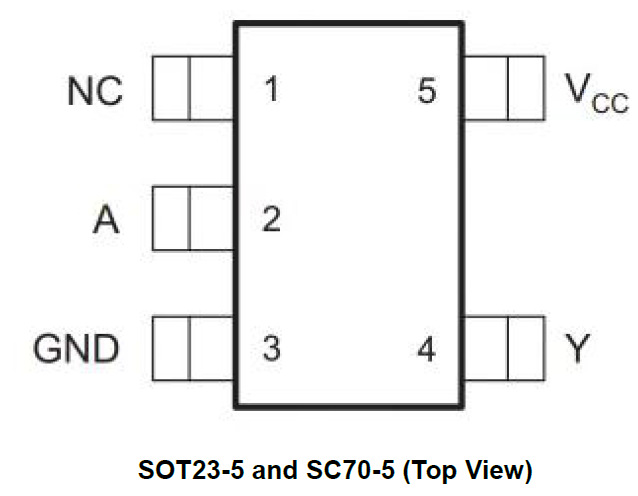
The PJ74LVC1G17 is a  Single Bus Buffer Gate with 3-State Output. The device is designed for 1.65 V to 5.5 V for VCC operation, it can be driven from either 3.3 V or 5 V devices. This feature allows the use of these devices as translators in mixed 3.3 V and 5 V environments. The PJ74LVC1G17 device contains one buffer and performs the Boolean function Y = A. The CMOS device has high output drive while maintaining low static power dissipation over a broad VCC operating range. The PJ74LVC1G17 is available in SOT23-5 and SC70-5 packages.

Product Specifications

Recommended Operating Conditions

Drag the table to view the full information.

Supply voltage
VCC
Operating
1.65
5.5
V
Data retention only
1.5
Input voltage
VI
0
5.5
V
Output voltage
VO
VCC
V
High-level output current
IOH
VCC = 1.65 V
-4
mA
VCC = 2.3 V
-8
VCC = 3 V
-16
VCC = 3 V
-24
VCC = 4.5 V
-32
Low-level output current
IOL
VCC = 1.65 V
4
mA
VCC = 2.3 V
8
VCC = 3 V
16
VCC = 3 V
24
VCC = 4.5 V
32
Operating temperature
TA
-40
125
°C

Key Electrical Characteristics

Drag the table to view the full information.

Parameter
Symbol
Test Conditions
Min
Typ
Max
Units
Positive-going input threshold voltage
VT+
VCC = 1.65 V
0.76
1.13
V
VCC = 2.3 V
1.08
1.56
VCC = 3 V
1.48
1.92
VCC = 4.5 V
2.19
2.74
VCC = 5.5 V
2.65
3.33
Negative-going input threshold voltage
VT-
VCC = 1.65 V
0.35
0.59
V
VCC = 2.3 V
0.56
0.88
VCC = 3 V
0.89
1.2
VCC = 4.5 V
1.51
1.97
VCC = 5.5 V
1.88
2.4
Hysteresis Voltage
△VT
VCC = 1.65 V
0.36
0.64
V
VCC = 2.3 V
0.45
0.78
VCC = 3 V
0.51
0.83
VCC = 4.5 V
0.58
0.93
VCC = 5.5 V
0.69
1.04
High-level output voltage
VOH
VCC = 1.65~5.5 V, IOH = 100 μA
VCC-0.1
V
VCC = 1.65 V, IOH = 4 mA
1.2
VCC = 2.3 V, IOH = 8 mA
1.9
VCC = 3 V, IOH = 16 mA
2.4
VCC = 3 V, IOH = 24 mA
2.3
VCC = 4.5 V, IOH = 32 mA
3.8
Low-level output voltage
VOL
VCC = 1.65~5.5 V, IOL = 100 μA
0.1
V
VCC = 1.65 V, IOL = 4 mA
0.45
VCC = 2.3 V, IOL = 8 mA
0.3
VCC = 3 V, IOL = 16 mA
0.4
VCC = 3 V, IOL = 24 mA
0.55
VCC = 4.5 V, IOL = 32 mA
0.55
Input leakage current
IL
VIN = 5.5 V or GND, VCC = 0~5.5 V
±5
μA
Power off leakage current
IOFF
VIN or GND, VCC = 0~5.5 V
±10
μA
Quiescent supply current
IQ
VIN = VCC or GND, IOUT = 0, VCC = 1.65~5.5 V
10
μA
Additional quiescent supply current per input pin
△IQ
VCC = 3~5.5 V, one input at VCC-0.6 V, other input at VCC or GND
500
μA

Product added!

Go To List