Signal Chain ICs

PJ72617

Datasheet
Add to Consultation List

Product Description

Level Translating FM+ I2C-bus Repeater

Product Features

2 channel, bidirectional translator for SDA and SCL in mixed-mode I2C applications
I2C and SMBus compatible
Voltage level translation from 0.8V to 5.5V and from 2.2V to 5.5V
Port A operating supply voltage range of 0.8V to 5.5V with normal levels
Port B operating supply voltage range of 2.2V to 5.5V with static offset level
5V tolerant I2C-bus and enable pins
0Hz to 1000kHz clock frequency (the maximum system operating frequency may be less than 1000kHz because of the delays added by the repeater)
Active HIGH repeater enable input referenced to VCCB
Open-drain input/outputs
Latching free operation
Supports arbitration and clock stretching across the repeater
Accommodates Standard-mode, Fast-mode and Fast-mode Plus I2C-bus devices, SMBus (standard and high power mode), PMBus and multiple masters
Powered-off high-impedance I2C-bus pins

Product Introduction

Product Specifications

Consultation List

Product Introduction

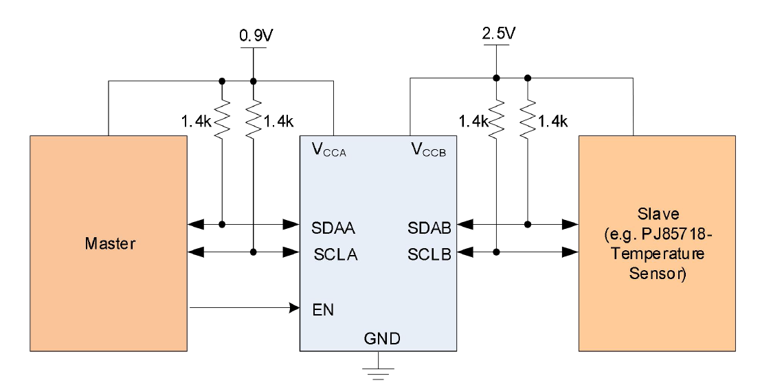
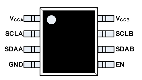
The PJ72617 is a CMOS integrated circuit that provides level shifting between low voltage (0.8V to 5.5V) and higher voltage (2.2V to 5.5V) Fast-mode Plus (FM+) I2C-bus or SMBus applications. While retaining all the operating modes and features I2C-bus system during the level shifts, it also permits extension of the I2C-bus by providing bidirectional buffering for both the data (SDA) and the clock (SCL) lines, thus enabling two buses of 540 pf at 1 MHz or up to 4000 pf at lower speeds. Using the PJ72617 enables the system designer to isolate two halves of a bus for both voltage and capacitance. The SDA and SCL pins are overvoltage tolerant and are high-impedance when the PJ72617 is unpowered. Available Package: MSOP-8, SOP-8

Product Specifications

Recommended Operating Conditions

Drag the table to view the full information.

Parameter
Symbol
Value
Unit
Supply voltage port A
VCCA
0.8 to 5.5
V
Supply voltage port B
VCCB
2.2 to 5.5
V
Operating free-air temperature
TA
-40 to 85
°C

Key Electrical Characteristics

Drag the table to view the full information.

Parameter
Symbol
Test Conditions
Min
Typ
Max
Unit
Supplies
Supply voltage port A
VCCA
-
0.8
-
5.5
V
Supply voltage port B
VCCB
-
2.2
-
5.5
V
Supply current port A
ICCA
VCCA = 0.95V
-
-
8
μA
Supply current port A
ICCA
VCCA = 5.5V
-
-
50
μA
Port B HIGH-level ,supply current
ICCHB
VCCB = 5.5V;SDAn = SCLn = VCCn
-
1.5
2.5
mA
Port B LOW-level supply current
ICCLB
VCCB = 5.5V; one SDA and one SCL = GND; other SDA and SCL open (with pull-up resistors)
-
1.7
2.9
mA
Input and output SDAB and SCLB
High-level input voltage
VIH
-
0.7*VCCB
-
5.5
V
Low-level input voltage
VIL
-
-0.5
-
0.4
V
Input clamp voltage
VIK
II = –18 mA;
-1.2
-
-0.3
V
Low-level output voltage
VOL
IOL =150uA at VCCB=2.2V
0.47
-
-
V
Low-level output voltage
VOL
IOL =13mA at VCCB=2.2V
0.54
0.63
V
Input leakage current
ILI
VI = 5.5V
-1
-
+1
μA
Differencebetween LOW-leveloutputand LOW-level inputvoltage
VOL - VIL
VOLat IOL=1mA; guaranteedbydesign
60
90
160
mV
Input and output SDAA and SCLA
Low-level input voltage
VIL
-
-0.5
-
0.25*VCCA
V
High-level input voltage
VIH
-
0.7*VCCA
-
5.5
V
Input clamp voltage
VIK
II = –18 mA;
-1.2
-
-0.3
V
Low-level output voltage
VOL
IOL =13mA at VCCB=2.2V
-
0.1
0.2
V
Input leakage current
ILI
VI = 5.5V
-1
-
+1
μA
Enable
LOW-level input voltage
VIL
-
-0.5
-
0.3*VCCB
V
HIGH-level input voltage
VIH
-
0.7*VCCB
-
5.5
V
LOW-level input current on pin EN
IIL(EN)
VI = 0.2V, EN; VCCB = 2.2V
-18
-7
-4
μA
Input leakage current
ILI
VI = VCCB
-1
-
+1
μA

Product added!

Go To List