Signal Chain ICs

PJ74LVC2G07

Datasheet
Add to Consultation List

Product Description

Dual Buffer and Driver With Open-Drain Outputs
In a SOT23-6 and SC70-6 Package

Product Features

WideSupply Voltage Range : 1.65 V to 5.5 V
Max.TPDof 3.7 ns at VCC = 3.3 V
LowPowerConsumption, 10 μA(Max. ICC)
-24mAOutput Drive at VCC = 3.3 V
Typical VOLP (Output Ground Bounce) < 0.8 V at VCC = 3.3 V, TA = 25°C
Typical VOHV (Output VOHUndershoot) > 2 V at VCC = 3.3 V, TA = 25°C
Support Translation-Up and Down
Ioff Supports Live Insertion, Partial-Power Down Mode, and Back-Drive Protection
Latch-Up Performance Exceeds 100 mAPer JESD 78, Class II
ESDProtection Exceeds JESD 22:2000VHuman-BodyModel(A114-A),1000VCharged-Device Model (C101)
Operating temperature Range :-40°C to 125°C

Product Introduction

Product Specifications

Consultation List

Product Introduction

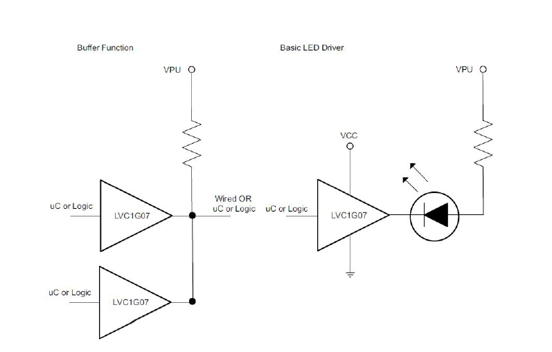
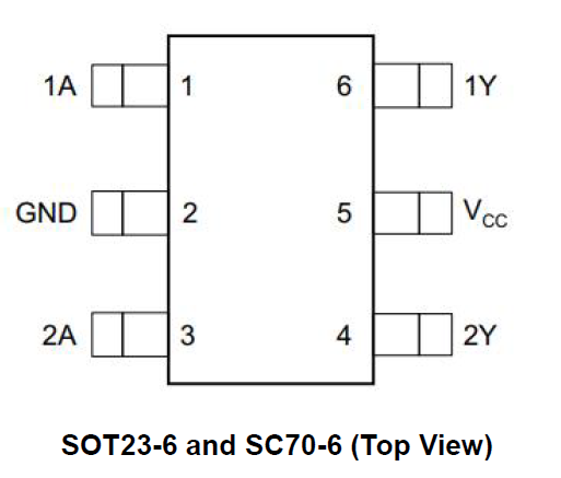
This dual buffer and driver is designed for 1.65 V to 5.5 V VCC operation. The output of PJ74LVC2G07 device is open drain and can be connected to other open-drain outputs to implement active-low wired-OR or active-high wired-AND functions. The maximum sink current is 32 mA. This device is fully specified for partial-power down applications using Ioff. The Ioff circuitry disables the outputs, preventing damaging current backflow through the device when it is powered down. The PJ74LVC2G07 is available in SOT23-6 and SC70-6 packages.

Product Specifications

RecommendedOperatingConditions

Drag the table to view the full information.

Parameter
Symbol
Test Conditions
Min
Max
Units
Supply voltage
VCC​
Operating
1.65
5.5
V
Supply voltage
VCC​
Data retention only
1.5
-
V
Input voltage
VI​
0
5.5
V
Output voltage
VO​
0
5.5
V
High-level input voltage
VIH​
VCC​=1.65 V to 1.95 V
0.65×VCC​
-
V
High-level input voltage
VIH​
VCC​=2.3 V to 2.7 V
1.7
-
V
High-level input voltage
VIH​
VCC​=3 V to 3.6 V
2
-
V
High-level input voltage
VIH​
VCC​=4.5 V to 5.5 V
0.7×VCC​
-
V
Low-level input voltage
VIL​
VCC​=1.65 V to 1.95 V
-
0.35×VCC​
V
Low-level input voltage
VIL​
VCC​=2.3 V to 2.7 V
-
0.7
V
Low-level input voltage
VIL​
VCC​=3 V to 3.6 V
-
0.8
V
Low-level input voltage
VIL​
VCC​=4.5 V to 5.5 V
-
0.3×VCC​
V
Low-level output current
IOL​
VCC​=1.65 V
-
4
mA
Low-level output current
IOL​
VCC​=2.3 V
-
8
mA
Low-level output current
IOL​
VCC​=3 V
-
16
mA
Low-level output current
IOL​
VCC​=3 V
-
24
mA
Low-level output current
IOL​
VCC​=4.5 V
-
32
mA
Input transition rise or fall rate
ΔT/ΔV
VCC​=1.8 V ±0.15 V, 2.5 V ±0.2 V
-
20
ns/V
Input transition rise or fall rate
ΔT/ΔV
VCC​=3.3 V ±0.3 V
-
10
ns/V
Input transition rise or fall rate
ΔT/ΔV
VCC​=5.0 V ±0.5 V
-
5
ns/V
Operating temperature
TA​
-
-40
125
°C

Key Electrical Characteristics

Drag the table to view the full information.

Parameter
Symbol
Test Conditions
Min
Max
Units
Low-level output voltage
VOL​
VCC​=1.65 V to 5.5 V, IOL​=100 μA
-
0.1
V
Low-level output voltage
VOL​
VCC​=1.65 V, IOL​=4 mA
-
0.45
V
Low-level output voltage
VOL​
VCC​=2.3 V, IOL​=8 mA
-
0.3
V
Low-level output voltage
VOL​
VCC​=3 V, IOL​=16 mA
-
0.4
V
Low-level output voltage
VOL​
VCC​=3 V, IOL​=24 mA
-
0.55
V
Low-level output voltage
VOL​
VCC​=4.5 V, IOL​=32 mA
-
0.55
V
Input leakage current
IL​
VI​=5.5 V or GND, VCC​=0 V to 5.5 V
-
±5
μA
Power off leakage current
IOFF​
VI​ or GND, VCC​=0 V to 5.5 V
-
±10
μA
Supply current
ICC​
VI​=VCC​ or GND, IOUT​=0, VCC​=1.65 V to 5.5 V
-
10
μA
Additional supply current per input pin
ΔICC​
VCC​=3 V to 5.5 V, one input at VCC​−0.6 V, other input at VCC​ or GND
-
500
μA

Product added!

Go To List