metawells
Product Description
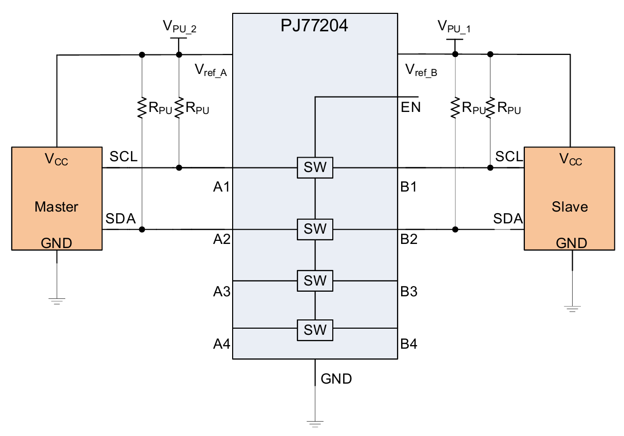
4-channel Auto-Bidirectional Multi-Voltage Level Translator
Product Features
Provides bidirectional voltage translation with no direction pin
Supports up to 100MHz up translation and greater than 100MHz down translation at ≤ 30pf cap load and up to 40MHz up/down translation at 50pf cap load
Allows voltage-level translation between :0.85V and 1.8V, 2.5V, 3.3V, or 5V,1.2V and 1.8V, 2.5V, 3.3V, or 5V,1.8V and 2.5V, 3.3V, or 5V,2.5V and 3.3V, or 5V,3.3V and 5V
Low standby current
5V tolerance I/O port to support TTL
Low Ron provides less signal distortion
High-impedance I/O pins for EN = Low
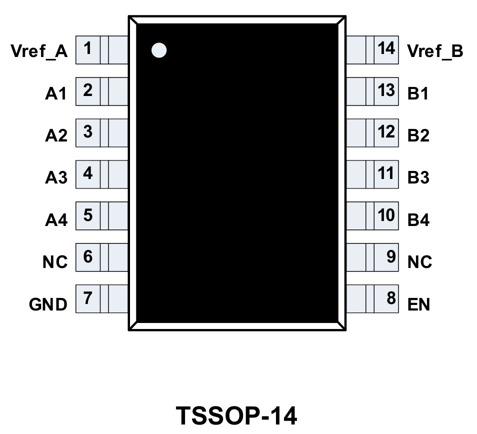
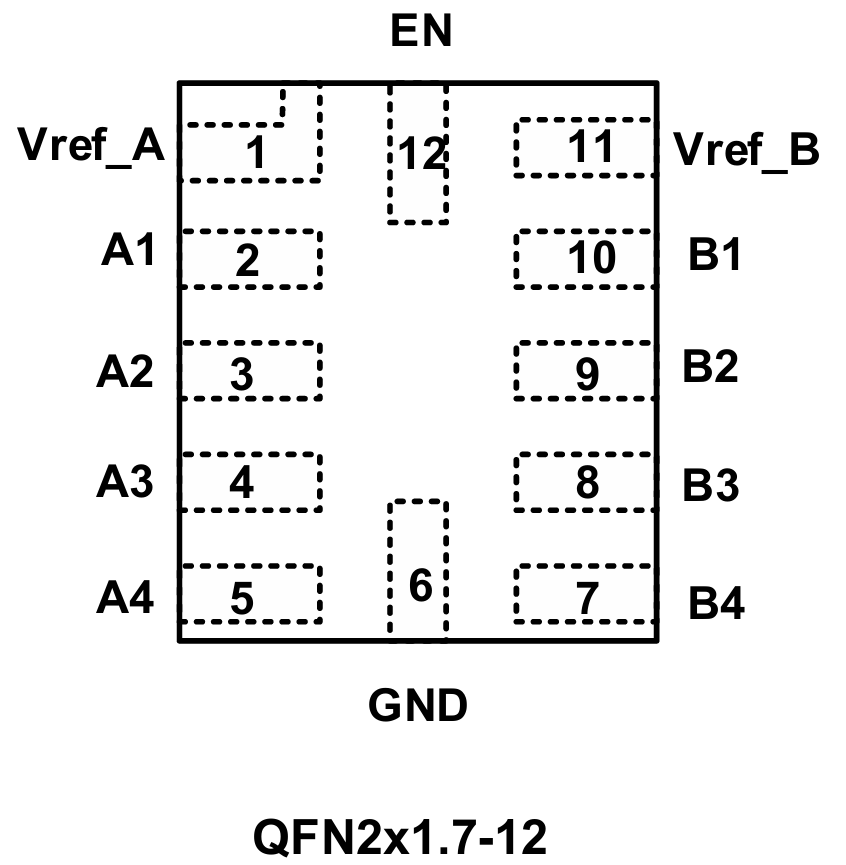
Flow-through pinout for easy PCB trace routing
Latch-up performance >200mA per JESD 17
-40°C to 125°C Operating temperature range
Applications
Product Specifications
Recommended Operating Conditions
Drag the table to view the full information.
Parameter
Symbol
Value
Unit
Input/output Voltage
VI/O
0 to 5.5
V
Reference Voltage A
Vref_A
0 to 5.5
V
Reference Voltage B
Vref_B
0 to 5.5
V
Enable input Voltage
EN
0 to 5.5
V
Max pass Switch Current
I_PASS
64
mA
Operating Ambient Temperature
TA
-40~125
°C
Key Electrical Characteristics
Drag the table to view the full information.
Parameter
Symbol
Test conditions
MIN
TYP
MAX
Unit
Input Clamp Voltage
V_IK
II = –18mA, EN = 0V
-1.2
-
-
V
Input Leakage Current
I_IH
VI = 5V, EN = 0V
-
-
5
uA
Leakage from Vref_B to Vref_A
Icc_BA
Vref_B=3.3V, Vref_A=1.8V,
VEN = Vref_A, IO = 0,
VI = 3.3 V or GND
-
-
3.5
uA
Total Current
through GND
Icc_A+Icc_B
Vref_B=3.3V, Vref_A=1.8V,
VEN = Vref_A, IO = 0,
VI = 3.3 V or GND
-
0.2
-
uA
Control pin current
Vref_B=5.5V, Vref_A=4.5V,
VEN = 0 to Vref_A, IO = 0
Vref_B=5.5V, Vref_A=4.5V,
-
-
±1
uA
Power off
leakage current
Ioff
Vref_B=Vref_A=0V,
VEN = GND, IO = 0,
VI = 5V or GND
-
-
±1
uA
Input Capacitance
Ci_(ref_A/ref_B)
VI = 3V or 0
-
17
-
pf
Input Capacitance
Ci_(EN)
VI = 3V or 0
-
7
-
pf
Off Capacitance
Cio(off)
VO = 3V or 0, EN = 0V
-
3
6
pf
On Capacitance
Cio(on)
VO = 3V or 0, EN = 3V
-
10
13
pf
High-level input voltage
V_IH(EN)
Vref_A=1V to 1.5V
0.8×Vref_ A
-
-
V
High-level input voltage
V_IH(EN)
Vref_A=1.5V to 4.5V
0.7×Vref_ A
-
-
V
Low-level input voltage
V_IL(EN)
Vref_A=1V to 4.5V
-
-
0.3×Vref_ A
V
Input transition rise or fall rate for EN pin
Δt/Δv(EN)
-
-
10
-
ns/V
On-state resistance
Ron
VI = 1.0V, IO =10mA, EN = Vref_A=1.8V,Vref_B=3.3V
-
8
20
ohm
On-state resistance
Ron
VI = 0, IO =10mA, EN = Vref_A=1V Vref_B=1.8V
-
6
15
ohm
On-state resistance
Ron
VI = 0, IO =10mA, EN = Vref_A=1V Vref_B=3.3V
-
6
15
ohm
On-state resistance
Ron
VI = 1.8V, IO =15mA, EN = Vref_A=3.3V,Vref_B=5V
5
10
ohm
On-state resistance
Ron
VI = 0, IO =32mA, EN = Vref_A=2.5V Vref_B=5V
4
8
ohm
On-state resistance
Ron
VI = 0, IO =64mA, EN = Vref_A=3.3V Vref_B=5V
3
6
ohm
On-state resistance
Ron
VI = 0, IO =64mA, EN = Vref_A=1.8V Vref_B=5V
4
10
ohm
On-state resistance
Ron
VI = 0, IO =32mA, EN = Vref_A=1.0V Vref_B=5V
6
15
ohm
On-state resistance
Ron
VI = 0, IO =32mA, EN = Vref_A=1.8V Vref_B=5V
4
8
ohm
Product added!


