電源轉換

PJ60221

資料表
加入諮詢清單

產品描述

Dual Gate Driver

產品特點

5V ±5% Power supply
Drain Voltage Range 1.0V to 20V
Internal Gate Voltage Charge Pump
Controlled Turn on Delay
Controlled Load Discharge Rate
Controlled Turn on Slew Rate
Stable Slew Rate(±2% Typ.) over Temperature
Pb-Free/Halogen-Free/RoHS compliant
DFN2X2-8

產品介紹

產品規格

相關檔案

諮詢清單

產品介紹

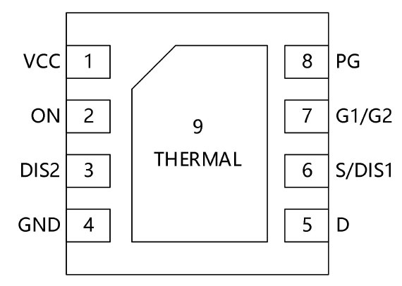
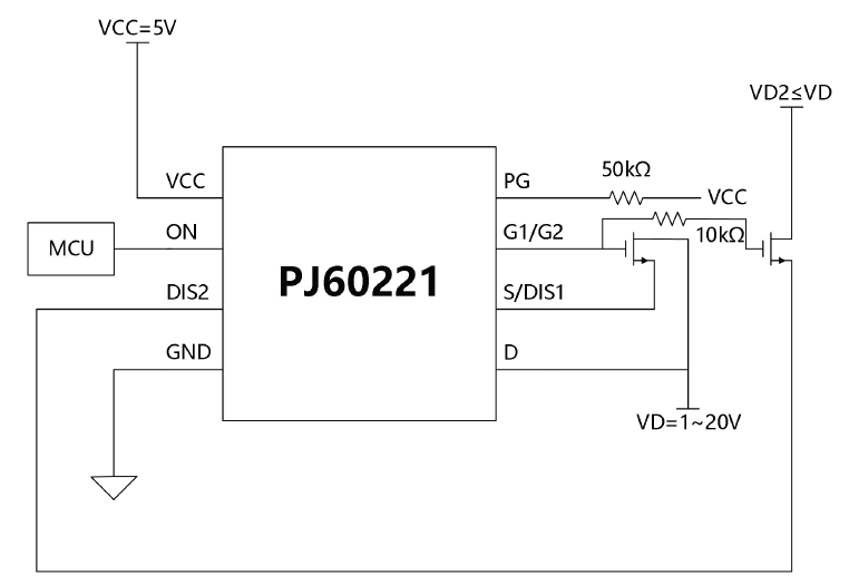
The PJ60221 N-Channel FET Gate Driver is used for controlling a delayed turn on and ramping slew rate (1.3V/ms, typ) of the source voltage on N-Channel FET switches from a CMOS logic level input. The PJ60221 integrates a charge pump internally, significantly reducing static power consumption. The quiescent current <5μA (typ) in standby state. Intended as a supporting control element for switched voltage rails in energy efficient, advanced power management systems, the PJ60221 also integrates circuits to discharge opened switched voltage rails. Furthermore, the PJ60221 is equipped with a built-in Power Good module to monitor whether the external N-FET is working properly.

產品規格

Recommended Operating Conditions

拖曳表格以查看完整資訊。

Parameter
Specification
Operating Temperature(TA)
-40°C~125°C
Continuous Supply Voltage (VCC)
4.75V~5.25V
Junction Temperature (TJ)
-40°C~125°C

Key Electrical Characteristics

拖曳表格以查看完整資訊。

Parameter
Condition
Specification
Quiescent Current
VG not ramping FET = ON
15uA (Typ.)
Quiescent Current
VG not ramping FET = OFF to ON
200uA (Typ.)
FET Drain Voltage
1V~20V
Gate - Source Voltage
8V~11V
FET Gate Capacitance
500pF~18000pF
Internal Discharge Resistor
Nominal discharge time of ~100ms 10mA max rate
400Ω (Typ.)
HIGH – Level input voltage
2.4V~5.5V
LOW – Level input voltage
<0.4V
Gate Drive Sink Current
VG = 5V
400uA (Min)
Gate Drive Source Current
32uA (Min)

相關檔案

技術資料

No.
項目
檔案格式
下載

PJ60221_Datasheet

PDF

產品已加入!

前往清單