訊號處理

PJ74LVC1G06

資料表
加入諮詢清單

產品描述

Single Inverter Buffer/Driver With Open-Drain Output
In a SOT23-5 and SC70-5 Package

產品特點

Supports 5-V VCC Operation
Input and Open-Drain Output Accept Voltage up to 5.5V
Max Tpd of 4.5 ns at 3.3 V
Low Power Consumption, 10-μA Max ICC
±24-mA Output Drive at 3.3 V for open-drain devices
IOFF Supports Partial-Power-Down Mode and Back-Drive
Latch-Up Performance Exceeds 100 mA Per JESD 78, Class II
Can Be Used For Up or Down Translation
Schmitt Trigger Action on All Ports
ESD Protection Exceeds JESD 22:2000-V Human-Body Model (A114-A),1000-V Charged-Device Model (C101)

產品介紹

產品規格

相關檔案

諮詢清單

產品介紹

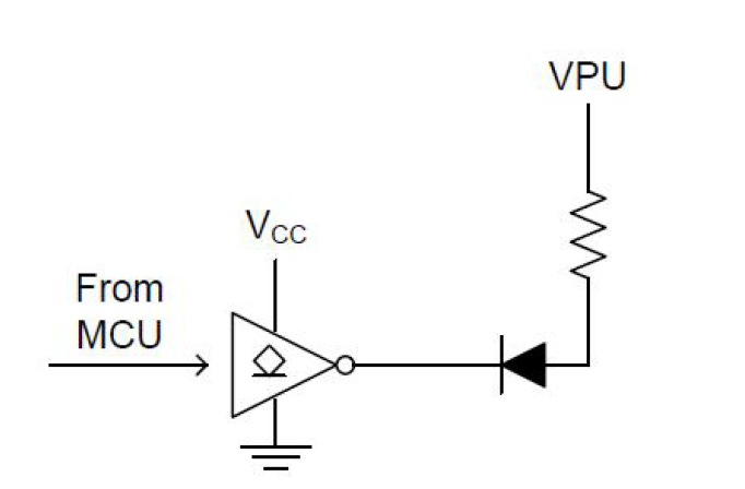
This single inverter buffer and driver is designed for 1.65-V to5.5-V VCC operation. The output of the PJ74LVC1G06 device is open-drain and can be connected to other open-drain outputs to implement active-low wired-OR or active-high wired-AND functions. The maximum sink current is 32mA. This device is fully specified for partial- power-down applications using IOFF circuitry disables the outputs when the device is powered down. This inhibits current backflow into the device which prevents damage to the device.

產品規格

Recommended Operating Conditions

拖曳表格以查看完整資訊。

Parameter
Symbol
Test Conditions
Min
Max
Units
Supply voltage
VCC
Operating
1.65
5.5
V
Data retention only
1.5
-
V
Input voltage
VI
0
5.5
V
Output voltage
VO
5.5
V
High- level input voltage
VIH
VCC = 1.65V to 1.95V
0.65 x VCC
-
V
High- level input voltage
VIH
VCC = 2.3V to 2.7V
1.7
-
V
High- level input voltage
VIH
VCC = 3V to 3.6V
2
-
V
High- level input voltage
VIH
VCC = 4.5V to 5.5V
0.7 x VCC
-
V
Low- level input voltage
VIL
VCC = 1.65V to 1.95V
-
0.35 x VCC
V
Low- level input voltage
VIL
VCC = 2.3V to 2.7V
-
0.7
V
Low- level input voltage
VIL
VCC = 3V to 3.6V
-
0.8
V
Low- level input voltage
VIL
VCC = 4.5V to 5.5V
-
0.3 x VCC
V
Low- level output current
IOL
VCC = 1.65V
-
4
mA
Low- level output current
IOL
VCC = 2.3V
-
8
mA
Low- level output current
IOL
VCC = 3V
-
16
mA
Low- level output current
IOL
VCC = 3V
-
24
mA
Low- level output current
IOL
VCC = 4.5V
-
32
mA
Input transition rise or fall rate
△T/△V
VCC = 1.8V±0.15V,2.5V±0.2V
-
20
ns/V
Input transition rise or fall rate
△T/△V
VCC = 3.3V±0.3V
-
10
ns/V
Input transition rise or fall rate
△T/△V
VCC = 5V±0.5V
-
5
ns/V
Operating temperature
TA
-40
125
°C

Key Electrical Characteristics

拖曳表格以查看完整資訊。

Parameter
Symbol
Test Conditions
Min
Max
Unit
Low- level output voltage
VOL
VCC = 1.65~5.5V, IOL= 100μA
-
0.1
V
Low- level output voltage
VOL
VCC = 1.65V, IOL= 4mA
-
0.45
V
Low- level output voltage
VOL
VCC = 2.3V, IOL= 8mA
-
0.3
V
Low- level output voltage
VOL
VCC = 3V, IOL= 16mA
-
0.4
V
Low- level output voltage
VOL
VCC = 3V, IOL= 24mA
-
0.55
V
Low- level output voltage
VOL
VCC = 4.5V, IOL= 32mA
-
0.55
V
Inflection-point current
Il
VIN= 5.5V or GND, VCC= 0~5.5V
-
±1
μA
Power off leakage current
IOFF
VI or VO = 5.5V, VCC=0V
-
±10
μA
Supply current
ICC
VI= 5.5V or GND, IOUT=0, VCC=1.65~5.5V
-
10
μA
Additional supply current per input pin
△ICC
VCC=3~5.5V, one input at VCC-0.6V, other input at VCC or GND
-
500
μA

相關檔案

技術資料

No.
項目
檔案格式
下載

PJ74LVC1G06_Datasheet

PDF

產品已加入!

前往清單